|
|
|
PDF XC9253R Data sheet ( Hoja de datos )
| Número de pieza | XC9253R | |
| Descripción | Synchronous Step-Down DC/DC Converter | |
| Fabricantes | Torex Semiconductor | |
| Logotipo | ||
Hay una vista previa y un enlace de descarga de XC9253R (archivo pdf) en la parte inferior de esta página. Total 13 Páginas | ||
|
No Preview Available !
XC9253R Series
Synchronous Step-Down DC/DC Converter
ETR0528_003
GreenOperation Compatible
GENERAL DESCRIPTION
The XC9253R series is a group of synchronous-rectification type DC/DC converters with a built-in 0.6 P-channel driver
transistor and 0.7 N-channel switching transistor, designed to allow the use of ceramic capacitors. The ICs enable a high
efficiency, stable power supply with an output current of 500mA to be configured using only a coil and two capacitors
connected externally. Minimum operating voltage is 2.0V~6.0V. Output voltage is 3.3V(accuracy: 2.0%). With the built-in
oscillator, oscillation frequency is set to 600kHz. As for operation mode, the XC9253R series is automatic PWM/PFM
switching control allowing fast response, low ripple and high efficiency over the full range of load (from light load to high
output current conditions).
The soft start and current control functions are internally optimized. During standby, all circuits are shutdown to reduce
current consumption to as low as 1.0 A or less. With the built-in UVLO (Under Voltage Lock Out) function, the internal
P-channel driver transistor is forced OFF when input voltage becomes 1.4V or lower. Two types of package, SOT-25 and
USP-6B, are available.
APPLICATIONS
Smart phones / Mobile phones
Bluetooth
Mobile devices / terminals
Portable game consoles
Digital still cameras / Camcorders
Note PCs / Tablet PCs
FEATURES
P-Ch Driver Tr. Built-In
N-Ch DriverTr. built-in
Input Voltage Range
Output Voltage Range
Low Power Consumption
Control Method
High Efficiency
: ON resistance 0.6
: ON resistance 0.7
: 2.0V~6.0V
: 3.3V
: 15 A (TYP.) (VIN=3.6V)
: PWM/PFM Automatic
: 92% (TYP.)
(VIN=4.5V, VOUT=3.3V, IOUT=100mA)
Output Current
: 500mA
Oscillation Frequency
: 600kHz ( 15%)
Low Output Ripple
: 10mV
Maximum Duty Ratio
: 100%
Operating Ambient Temperature : -40
+85
Packages
: SOT-25, USP-6B
Soft-Start Circuit Built-In
Current Limiter Circuit Built-In (Constant Current & Latching)
Low ESR Ceramic Capacitor Compatible
* Performance depends on external components and wiring on the PCB
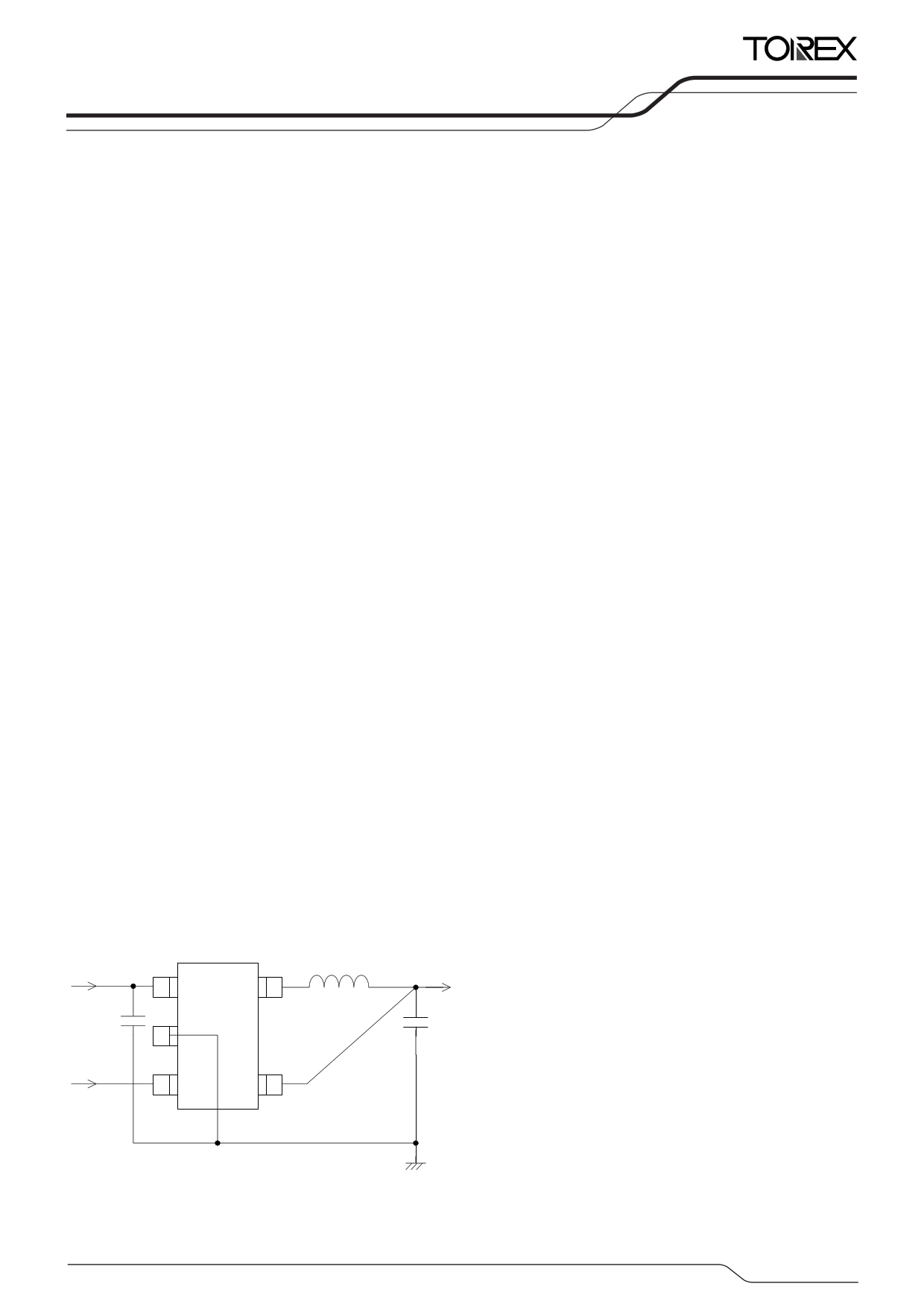
TYPICAL APPLICATION CIRCUIT
V IN
C IN
(ceramic)
CE
1 VIN
Lx 5
2 VSS
CE
3
VOUT 4
L
V OUT
500mA
CL
(ceramic)
1/13
1 page 
TYPICAL APPLICATION CIRCUIT
L
V IN
1 VIN
Lx 5
V OUT
500mA
C IN
(ceramic)
CE
2 VSS
CE
3
VOUT 4
CL
(ceramic)
XC9253R
Series
fosc=600kHz
L : 10 H
: 10 H
: 10 H
CIN : 4.7 F
CL : 10 F
(NR4018, TAIYO YUDEN)
(VLF4012A, TDK)
(CDRH4, SUMIDA)
(Ceramic)
(Ceramic)
OPERATIONAL EXPLANATION
The XC9253R series consists of a reference voltage source, ramp wave circuit, error amplifier, PWM comparator, phase
compensation circuit, output voltage adjustment resistors, P-channel MOSFET driver transistor, N-channel MOSFET switching
transistor for the synchronous switch, current limiter circuit, U.V.L.O. circuit and others. (See the block diagram above.) The
series ICs compare, using the error amplifier, the voltage of the internal voltage reference source with the feedback voltage
from the VOUT pin through split resistors, R1 and R2. Phase compensation is performed on the resulting error amplifier output,
to input a signal to the PWM comparator to determine the turn-on time during PWM operation. The PWM comparator
compares, in terms of voltage level, the signal from the error amplifier with the ramp wave from the ramp wave circuit, and
delivers the resulting output to the buffer driver circuit to cause the Lx pin to output a switching duty cycle. This process is
continuously performed to ensure stable output voltage. The current feedback circuit monitors the P-channel MOS driver
transistor current for each switching operation, and modulates the error amplifier output signal to provide multiple feedback
signals. This enables a stable feedback loop even when a low ESR capacitor, such as a ceramic capacitor, is used, ensuring
stable output voltage.
<Reference Voltage Source>
The reference voltage source provides the reference voltage to ensure stable output voltage of the DC/DC converter.
<Ramp Wave Circuit>
The ramp wave circuit determines switching frequency. The frequency is fixed internally as 600kHz. Clock pulses generated in
this circuit are used to produce ramp waveforms needed for PWM operation, and to synchronize all the internal circuits.
<Error Amplifier>
The error amplifier is designed to monitor output voltage. The amplifier compares the reference voltage with the feedback
voltage divided by the internal split resistors, R1 and R2. When a voltage lower than the reference voltage is fed back, the
output voltage of the error amplifier increases. The gain and frequency characteristics of the error amplifier output are fixed
internally to deliver an optimized signal to the mixer.
<Current Limit>
The current limiter circuit of the XC9253R series monitors the current flowing through the P-channel MOS driver transistor
connected to the Lx pin, and features a combination of the constant-current type current limit mode and the operation
suspension mode.
When the driver current is greater than a specific level, the constant-current type current limit function operates to turn off
the pulses from the Lx pin at any given timing.
When the driver transistor is turned off, the limiter circuit is then released from the current limit detection state.
At the next pulse, the driver transistor is turned on. However, the transistor is immediately turned off in the case of an over
current state.
When the over current state is eliminated, the IC resumes its normal operation.
The IC waits for the over current state to end by repeating the steps through . If an over current state continues for a
few msec and the above three steps are repeatedly performed, the IC performs the function of latching the OFF state of the
driver transistor, and goes into operation suspension mode. Once the IC is in suspension mode, operations can be resumed by
either turning the IC off via the CE pin, or by restoring power to the VIN pin. The suspension mode does not mean a complete
shutdown, but a state in which pulse output is suspended; therefore, the internal circuitry remains in operation. The
constant-current type current limit of the XC9253R series can be set at 700mA at typical. Besides, care must be taken when
laying out the PC Board, in order to prevent misoperation of the current limit mode. Depending on the state of the PC Board,
latch time may become longer and latch operation may not work. In order to avoid the effect of noise, the board should be laid
out so that capacitors are placed as close to the chip as possible.
Limit < mS
Limit > mS
Current Limit LEVEL
Iout
0mA
VOU T
VSS
LX
CE/M ODE
VIN
R estar t
5/13
5 Page 
PACKAGING INFORMATION
SOT-25
USP-6B
XC9253R
Series
USP-6B Reference Pattern Layout
USP-6B Reference Metal Mask Design
11/13
11 Page | ||
| Páginas | Total 13 Páginas | |
| PDF Descargar | [ Datasheet XC9253R.PDF ] | |
Hoja de datos destacado
| Número de pieza | Descripción | Fabricantes |
| XC9253R | Synchronous Step-Down DC/DC Converter | Torex Semiconductor |
| Número de pieza | Descripción | Fabricantes |
| SLA6805M | High Voltage 3 phase Motor Driver IC. |
Sanken |
| SDC1742 | 12- and 14-Bit Hybrid Synchro / Resolver-to-Digital Converters. |
Analog Devices |
|
DataSheet.es es una pagina web que funciona como un repositorio de manuales o hoja de datos de muchos de los productos más populares, |
| DataSheet.es | 2020 | Privacy Policy | Contacto | Buscar |