|
|
|
PDF MCP1632 Data sheet ( Hoja de datos )
| Número de pieza | MCP1632 | |
| Descripción | Low-Side PWM Controller | |
| Fabricantes | Microchip | |
| Logotipo | ||
Hay una vista previa y un enlace de descarga de MCP1632 (archivo pdf) en la parte inferior de esta página. Total 30 Páginas | ||
|
No Preview Available !
MCP1632
High-Speed, Low-Side PWM Controller
Features:
• High-Speed PWM Controller with Integrated
Low-Side MOSFET Driver
• Multiple Switching Frequency Options (fSW):
- 300 kHz
- 600 kHz
• Adjustable Reference Voltage Generator
• Adjustable Soft Start
• Internal Slope Compensation
• Shutdown Input Pin (EN)
• Low Operating Current: < 5 mA (typical)
• Undervoltage Lockout (UVLO) Protection
• Output Short Circuit Protection
• Overtemperature Protection
• Operating Temperature Range:
- -40°C to +125°C
Applications:
• Switch Mode Power Supplies
• Brick DC-DC Converters
• Battery Charger Applications
• LED Drivers
Related Literature:
• “MCP1632 300 kHz Boost Converter Demo Board
User’s Guide”, Microchip Technology Inc.,
DS20005252A, 2013
Description:
The MCP1632 high-speed PWM controller is a
pulse-width modulator developed for stand-alone power
supply applications. The MCP1632 includes a
high-speed analog control loop, a logic-level MOSFET
driver, an internal oscillator, a reference voltage
generator, and internal slope compensation. This high
level of integration makes it an ideal solution for
standalone SMPS applications. MCP1632 is suitable for
use in topologies requiring a low-side MOSFET control,
such as Boost, Flyback, SEPIC, Ćuk, etc. Typical
applications include battery chargers, intelligent power
systems, brick DC-DC converters, LED drivers. Due to
its low power consumption, the MCP1632 PWM
controller is recommended for battery-operated
applications.
The MCP1632 offers a Peak Current mode control in
order to achieve consistent performance regardless of
the topology of the power train or the operating
conditions. In addition, the MCP1632 can implement
the Voltage Mode Control for cost-sensitive solutions.
The MCP1632 PWM controller can be easily interfaced
with PIC microcontrollers in order to develop an
intelligent power solution.
Additional features include: UVLO, overtemperature
and overcurrent protection, shutdown capability (EN
pin) and an adjustable soft start option.
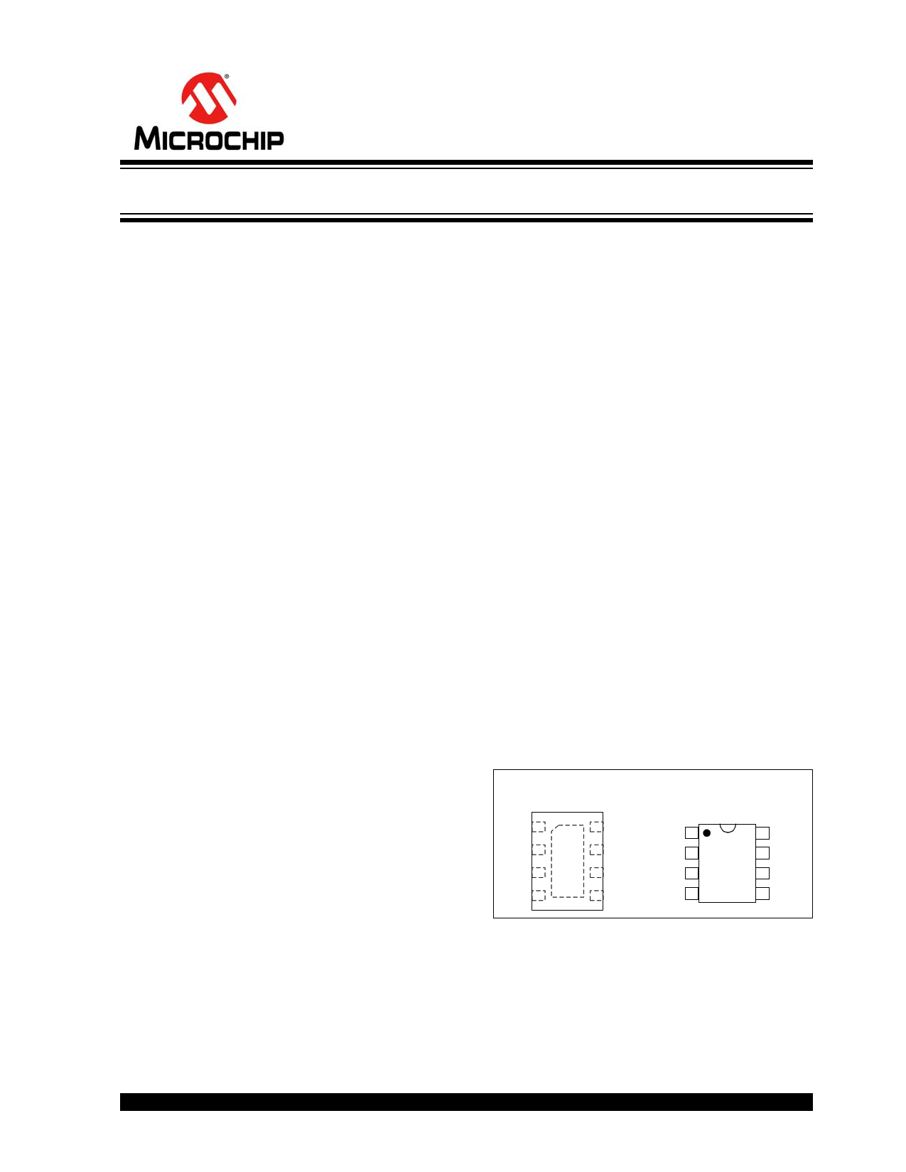
Package Type
8-Lead DFN
(2 mm x 3 mm)
8-Lead MSOP
COMP 1
8 VREF COMP 1
FB 2 EP 7 Vin
CS 3 9 6 VEXT
FB 2
CS 3
EN 4
5 GND
EN 4
8 VREF
7 VIN
6 VEXT
5 GND
2013 Microchip Technology Inc.
DS20005254A-page 1
1 page 
MCP1632
AC/DC CHARACTERISTICS (CONTINUED)
Electrical Specifications: Unless otherwise noted, VIN = 3.0V to 5.5V, FOSC = 300 kHz, CIN = 0.1 µF,
VIN for typical values = 5.0V, TA = -40°C to +125°C.
Parameters
Sym.
Min. Typ. Max. Units
Conditions
Error Amplifier
Source Current
ISOURCE
4
6 — mA VIN = 5V, VREF = 1.2V,
VFB = 1.0V, VCOMP = 2.0V,
Absolute Value
Current Sense Input
Maximum Current Sense
Signal
Blanking Time
Delay from CS to VEXT
VCS_MAX
TBLANK
TCS_VEXT
0.8
80
—
0.9 0.97
100 130
— 35
V Set by maximum error amplifier
clamp voltage, divided by 3
(Note 1)
ns Note 1
ns Excluding the blanking time
(Note 1)
Current Sense Input Bias
Current
ICS_B
— -0.1 — µA Note 1
PWM Section
Minimum Duty Cycle
DCMIN
Maximum Duty Cycle
DCMAX
Slope Compensation Ramp Generator
Ramp Amplitude
VRAMP
DC Offset Low
—
—
80
0.8
0.15
DC Offset High
— 1.12
Ramp Generator Output
Impedance
ZRG
5.5
—0
85 95
0.9 1
0.32 0.45
1.22 1.32
6 6.5
% VFB = VREF + 0.1V, VCS = GND
(Note 1)
%
VPP Refer to Section 4.6 “Slope
Compensation” for details.
V Refer to Section 4.6 “Slope
Compensation” for details.
V Refer to Section 4.6 “Slope
Compensation” for details.
k Refer to Section 4.6 “Slope
Compensation” for details.
Internal Driver
RDSon P-channel
RDSon N-channel
VEXT Rise Time
VEXT Fall Time
Protection Features
Undervoltage Lockout
Undervoltage Lockout
Hysteresis
Thermal Shutdown
Thermal Shutdown
Hysteresis
RDSon_P
RDSon_N
TRISE
TFALL
—
—
—
—
UVLO
UVLOHYS
TSHD
TSHD_HYS
2.6
50
—
—
10 30
7 30
— 18
— 18
— 2.9
110 180
150 —
20 —
ns CL = 100 pF
Typical for VIN = 3V (Note 1)
ns CL = 100 pF
Typical for VIN = 3V (Note 1)
V VIN falling,
VEXT low state when in UVLO
mV
°C Note 1
°C Note 1
Note 1: Ensured by design. Not production tested.
2013 Microchip Technology Inc.
DS20005254A-page 5
5 Page 
MCP1632
3.0 PIN DESCRIPTIONS
The descriptions of the pins are listed in Table 3-1.
TABLE 3-1:
DFN/MSOP
1
2
3
4
5
6
7
8
9
PIN FUNCTION TABLE
Name
COMP
FB
CS
EN
GND
VEXT
VIN
VREF
EP
Function
Error Amplifier Output
Error Amplifier Inverting Input
Current Sense Input
Enable Input
Circuit Ground
External Driver Output
Input Bias
Reference Voltage Input/Internal Constant Current Generator Output
Exposed Thermal Pad (EP); must be connected to GND
3.1 Error Amplifier Output (COMP)
COMP is the internal error amplifier output pin. External
compensation is connected from the FB pin to the
COMP pin for control-loop stabilization. Type II or III
compensation networks must be used depending on
the application. An internal voltage clamp is used to
limit the maximum COMP pin voltage to 2.7V (typical).
This clamp is used to set the maximum peak current in
the power system switch by setting a maximum limit on
the CS input for Peak Current Mode control systems.
3.2 Error Amplifier Inverting Input
(FB)
FB is the internal error amplifier inverting input pin. The
output (voltage or current) is sensed and fed back to
the FB pin for regulation. Inverting or negative
feedback is used.
3.3 Current Sense Input (CS)
This is the input for the switch current used for Peak
Current Mode control. A blanking period of 100 ns
(typical) for CS signal is provided to avoid leading edge
spikes that can cause false PWM reset. The normal
PWM duty cycle will be terminated when the voltage on
the CS pin (including the slope compensation ramp) is
equal to the output of the error amplifier divided by 3.
For Current Mode operation, the CS pin will control the
PWM output on a cycle-by-cycle basis. The internal
error amplifier output is clamped to 2.7V (nominal) and
divided by 3, so the maximum voltage of the CS pin is
0.9V. By limiting the inverting pin of the high-speed
comparator to 0.9V, a current sense limit is established
for all input bias voltage conditions (cycle-by-cycle
overcurrent protection). To avoid the instability of the
Peak Current Mode control when the duty cycle is
higher than 50%, a slope compensation ramp
generator is internally provided. This circuit will add to
the CS signal an artificially generated ramp to avoid
sub-harmonic oscillations. The amplitude of the slope
compensation ramp is adjustable with one external
resistor.
If this pin is left open, the PWM Controller will operate
in Voltage Mode Control. In this mode, the external
switching MOSFET transistor is not protected against
overcurrent conditions. Certain limitations related to the
stability of the closed-loop system must be taken into
account by the designer when the part operates in
Voltage Mode Control. Refer to Section 5.2
“Operation in Voltage Mode Control” for details
about the operation in Voltage Mode Control.
3.4 Enable Input (EN)
When this pin is connected to GND (logic “Low”) for
more than 50 µs (typical), the chip will go into
Shutdown state. A logic “High” enables the normal
operation of the MCP1632 device. When the device is
disabled, the VEXT output is held low. Do not let the EN
pin float. If not used, connect EN to VIN through a 10 k
resistor.
3.5 Circuit Ground (GND)
Connect the circuit ground to the GND pin. For most
applications, this should be connected to the analog
(quiet) ground plane. Effort should be made to
minimize the noise on this ground, as it can adversely
affect the cycle-by-cycle comparison between the CS
input and the error amplifier output.
3.6 External Driver Output (VEXT)
VEXT is the internal MOSFET driver output pin, used to
drive the external transistor. For high-power or high-side
drives, this output should be connected to the logic-level
input of an appropriate MOSFET driver. For low-power,
low-side applications, the VEXT pin can be used to
directly drive the gate of an N-channel MOSFET.
2013 Microchip Technology Inc.
DS20005254A-page 11
11 Page | ||
| Páginas | Total 30 Páginas | |
| PDF Descargar | [ Datasheet MCP1632.PDF ] | |
Hoja de datos destacado
| Número de pieza | Descripción | Fabricantes |
| MCP1630 | Pulse Width Modulator | Microchip Technology |
| MCP16301 | High-Voltage Input Integrated Switch Step-Down Regulator | Microchip |
| MCP16301H | High-Voltage Input Integrated Switch Step-Down Regulator | Microchip |
| MCP1630V | Pulse Width Modulator | Microchip |
| Número de pieza | Descripción | Fabricantes |
| SLA6805M | High Voltage 3 phase Motor Driver IC. |
Sanken |
| SDC1742 | 12- and 14-Bit Hybrid Synchro / Resolver-to-Digital Converters. |
Analog Devices |
|
DataSheet.es es una pagina web que funciona como un repositorio de manuales o hoja de datos de muchos de los productos más populares, |
| DataSheet.es | 2020 | Privacy Policy | Contacto | Buscar |