|
|
|
PDF MCP1662 Data sheet ( Hoja de datos )
| Número de pieza | MCP1662 | |
| Descripción | High-Voltage Step-Up LED Driver | |
| Fabricantes | Microchip | |
| Logotipo | ||
Hay una vista previa y un enlace de descarga de MCP1662 (archivo pdf) en la parte inferior de esta página. Total 28 Páginas | ||
|
No Preview Available !
MCP1662
High-Voltage Step-Up LED Driver with UVLO and Open Load Protection
Features
• 36V, 800 m Integrated Switch
• Up to 92% Efficiency
• Drive LED Strings in Constant Current
• 1.3A Peak Input Current Limit:
- ILED up to 200 mA @ 5.0V VIN, 4 White LEDs
- ILED up to 125 mA @ 3.3V VIN, 4 White LEDs
- ILED up to 100 mA @ 4.2V VIN, 8 White LEDs
• Input Voltage Range: 2.4V to 5.5V
• Feedback Voltage Reference: VFB = 300 mV
• Undervoltage Lockout (UVLO):
- UVLO @ VIN Rising: 2.3V, typical
- UVLO @ VIN Falling: 1.85V, typical
• Sleep Mode with 20 nA Typical Quiescent Current
• PWM Operation: 500 kHz Switching Frequency
• Cycle-by-Cycle Current Limiting
• Internal Compensation
• Open Load Protection (OLP) in the Event of:
- Feedback pin shorted to GND (prevent
excessive current into LEDs)
- Disconnected LED string (prevent overvoltage
to the converter’s Output and SW pin)
• Overtemperature Protection
• Available Packages:
- 5-Lead SOT-23
- 8-Lead 2x3 TDFN
Applications
• Two and Three-Cell Alkaline or NiMH/NiCd White
LED Driver for Backlighting Products
• Li-Ion Battery LED Lighting Application
• Camera Flash
• LED Flashlights and Backlight Current Source
• Medical Equipment
• Portable Devices:
- Handheld Gaming Devices
- GPS Navigation Systems
- LCD Monitors
- Portable DVD Players
General Description
The MCP1662 device is a compact, space-efficient,
fixed-frequency, non-synchronous step-up converter
optimized to drive LED strings with constant current
from a two- or three-cell alkaline or lithium Energizer®,
or NiMH/NiCd, or one-cell Lithium-Ion or Li-Polymer
batteries.
The device integrates a 36V, 800 m low-side switch,
which is protected by the 1.3A cycle-by-cycle inductor
peak current limit operation. All compensation and pro-
tection circuitry is integrated to minimize the number of
external components.
The internal feedback (VFB) voltage is set to 300 mV for
low power dissipation when sensing and regulating the
LED current. A single resistor sets the LED current.
The device features an Undervoltage Lockout (UVLO)
that avoids start-up with low inputs or discharged bat-
teries for two-cell-powered applications.
There is an open load protection (OLP) which turns off
the operation in situations when the LED string is acci-
dentally disconnected or the feedback pin is short-cir-
cuited to GND.
For standby applications (EN = GND), the device stops
switching, enters into Sleep mode and consumes
20 nA typical of input current.
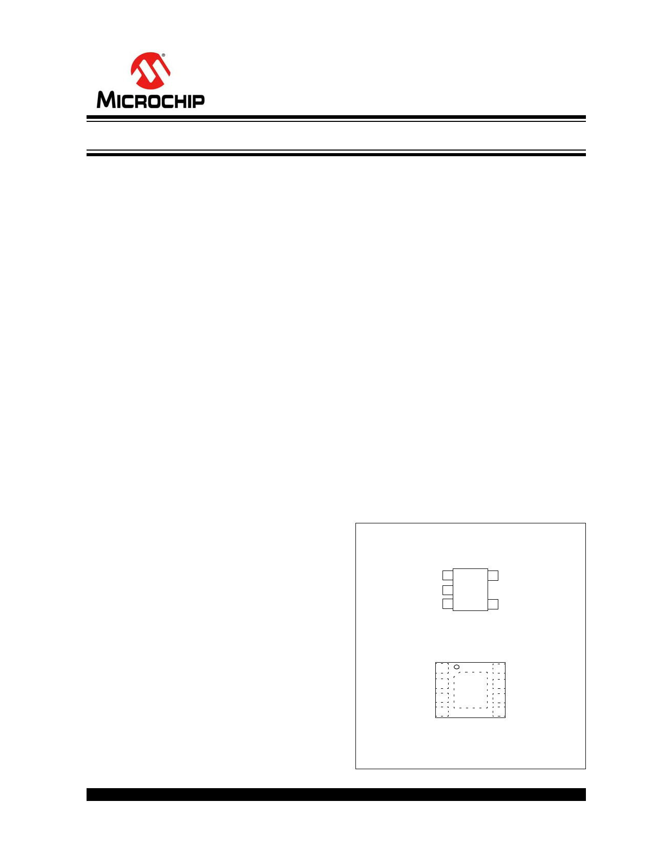
Package Types
MCP1662
SOT-23
SW 1
GND 2
VFB 3
5 VIN
4 EN
MCP1662
2x3 TDFN*
VFB 1
8 EN
SGND 2 EP 7 PGND
SW 3 9 6 NC
NC 4
5 VIN
* Includes Exposed Thermal Pad (EP); see
Table 3-1.
2014-2015 Microchip Technology Inc.
DS20005316E-page 1
1 page 
MCP1662
2.0 TYPICAL PERFORMANCE CURVES
Note:
The graphs and tables provided following this note are a statistical summary based on a limited number of
samples and are provided for informational purposes only. The performance characteristics listed herein
are not tested or guaranteed. In some graphs or tables, the data presented may be outside the specified
operating range (e.g., outside specified power supply range) and therefore outside the warranted range.
Note: Unless otherwise indicated: VIN = 3.3V, ILED = 20 mA, VOUT = 12V or 4 white LEDs (VF = 2.75V @ IF = 20 mA or
VF = 3.1V @ IF = 100 mA), CIN = COUT = 10 µF, X7R ceramic, L = 4.7 µH.
150
4 x wLED, L = 4.7 µH
125
100
RSET = 2.2ȍ
RSET = 3.2ȍ
75
50 RSET = 6.2ȍ
25 RSET = 15ȍ
0
2.3 2.7 3.1 3.5 3.9 4.3 4.7 5.1 5.5
Input Voltage (V)
FIGURE 2-1:
4 White LEDs, ILED vs. VIN.
100
90
80
70
60
50
40
30
20
10
0
0
VIN = 5.5V
VIN = 4.0V
VIN = 3.0V
L = 4.7 µH,
4 wLEDs
25 50 75 100 125 150 175 200 225 250
ILED (mA)
FIGURE 2-4:
ILED.
4 White LEDs, Efficiency vs.
120
100
4 x wLED, L = 4.7 µH, VIN = 3.3V
RSET = 3.2ȍ
80
60
RSET = 6.2ȍ
40
20 RSET = 15ȍ
0
-40 -25 -10 5 20 35 50 65 80 95 110 125
Ambient Temperature (oC)
FIGURE 2-2:
4 White LEDs, ILED vs.
Ambient Temperature.
100
90
80
70
60
50
40
30
20
10
0
0
VIN = 3.0V
VIN = 4.0V
VIN = 5.5V
L = 10 µH,
8 wLEDs
20 40 60 80 100 120 140 160
ILED (mA)
FIGURE 2-5:
ILED.
8 White LEDs, Efficiency vs.
120
8 x wLED, L = 10 µH, VIN = 4.2V
100
RSET = 3.2ȍ
80
60
RSET = 6.2ȍ
40
RSET = 15ȍ
20
0
-40 -25 -10 5 20 35 50 65 80 95 110 125
Ambient Temperature (oC)
FIGURE 2-3:
8 White LEDs, ILED vs.
Ambient Temperature.
300
250
200 2 wLEDs, L = 4.7 µH
5 wLEDs, L = 10 µH
150 4 wLEDs, L = 4.7 µH
100
8 wLEDs, L = 10 µH
50
0
2.3 2.7 3.1 3.5 3.9 4.3 4.7 5.1 5.5
Input Voltage (V)
FIGURE 2-6:
Maximum ILED vs. VIN.
2014-2015 Microchip Technology Inc.
DS20005316E-page 5
5 Page 
4.2.1 INTERNAL BIAS
The MCP1662 gets its bias from VIN. The VIN bias is
used to power the device and drive circuits over the
entire operating range.
4.2.2 START-UP
The MCP1662 is capable of starting from two alkaline
cells. MCP1662 starts switching at approximately 2.3V
typical for a light load current. Once started, the device
will continue to operate down to 1.85V, typical.
The start-up time is dependent on the LED’s current, on
the number of LEDs connected at output, and on the
output capacitor value (see Figure 2-10).
Due to the direct path from input to output, in the case
of pulsing enable applications (EN voltage switches
from low-to-high) the output capacitor is already
charged and the output starts from a value close to the
input voltage.
The internal oscillator has a delayed start to let the out-
put capacitor completely charge to the input voltage
value.
4.2.3
UNDERVOLTAGE LOCKOUT
(UVLO)
MCP1662 features an UVLO which prevents fault oper-
ation below 1.85V typical, which corresponds to the
value of two discharged alkaline batteries.
Essentially, there is a hysteresis comparator which
monitors VIN at the reference voltage derived from the
bandgap.
The device starts its normal operation at 2.3V typical
input, which corresponds to the voltage value of two
rechargeable Ni-MH or Ni-Cd cells. A hysteresis is set
to avoid input transients (temporary VIN drop), which
might trigger the lower UVLO threshold and restart the
device.
When the input voltage is below the UVLOSTART
threshold, the device is operating with limited specifica-
tion.
4.2.4 ENABLE PIN
The MCP1662 device enables switching when the EN
pin is set high. The device is put into Shutdown mode
when the EN pin is set low. To enable the boost con-
verter, the EN voltage level must be greater than 85%
of the VIN voltage. To disable the boost converter, the
EN voltage must be less than 7.5% of the VIN voltage.
MCP1662
4.2.4.1
Shutdown Mode.
Input to Output Path (EN = GND)
In Shutdown mode, the MCP1662 device stops switch-
ing and all internal control circuitry is switched off. The
input voltage will be bypassed to output through the
inductor and the Schottky diode.
While the device stops switching, VOUT is equal to the
output capacitor voltage, which slowly discharges on
the leak path (from VOUT to a value close to VIN) after
the LEDs are turned off.
In Shutdown mode, the current consumed by the
MCP1662 device from batteries is very low (below
50 nA over VIN range; see Figure 2-8).
4.2.5 PWM MODE OPERATION
The MCP1662 operates as a fixed-frequency, non-syn-
chronous converter. The switching frequency is main-
tained with a precision oscillator at 500 kHz.
Lossless current sensing converts the peak current sig-
nal to a voltage (VSENSE) and adds it to the internal
slope compensation (VRAMP). This summed signal is
compared to the voltage error amplifier output (VER-
ROR) to provide a peak current control signal (VPWM) for
the PWM. The slope compensation signal depends on
the input voltage. Therefore, the converter provides the
proper amount of slope compensation to ensure stabil-
ity. The peak limit current is set to 1.3A.
4.2.6 INTERNAL COMPENSATION
The error amplifier, with its associated compensation
network, completes the closed-loop system by compar-
ing the output voltage to a reference at the input of the
error amplifier and by feeding the amplified signal to the
control input of the inner current loop. The compensa-
tion network provides phase leads and lags at appropri-
ate frequencies to cancel excessive phase lags and
leads of the power circuit. All necessary compensation
components and slope compensation are integrated.
2014-2015 Microchip Technology Inc.
DS20005316E-page 11
11 Page | ||
| Páginas | Total 28 Páginas | |
| PDF Descargar | [ Datasheet MCP1662.PDF ] | |
Hoja de datos destacado
| Número de pieza | Descripción | Fabricantes |
| MCP1661 | High-Voltage Integrated Switch PWM Boost Regulator | Microchip |
| MCP1662 | High-Voltage Step-Up LED Driver | Microchip |
| Número de pieza | Descripción | Fabricantes |
| SLA6805M | High Voltage 3 phase Motor Driver IC. |
Sanken |
| SDC1742 | 12- and 14-Bit Hybrid Synchro / Resolver-to-Digital Converters. |
Analog Devices |
|
DataSheet.es es una pagina web que funciona como un repositorio de manuales o hoja de datos de muchos de los productos más populares, |
| DataSheet.es | 2020 | Privacy Policy | Contacto | Buscar |