|
|
|
PDF 34923 Data sheet ( Hoja de datos )
| Número de pieza | 34923 | |
| Descripción | Full-Bridge PWM Motor Driver | |
| Fabricantes | Freescale Semiconductor | |
| Logotipo | ||
Hay una vista previa y un enlace de descarga de 34923 (archivo pdf) en la parte inferior de esta página. Total 16 Páginas | ||
|
No Preview Available !
www.DataSheet4U.com
Freescale Semiconductor, Inc.
MOTOROLA
Order this document from Analog Marketing: MC34923/D
Rev 0, 05/2003
SEMICONDUCTOR TECHNICAL DATA
Preliminary Information
Full-Bridge PWM Motor Driver
Designed with Motorola’s advanced SMARTMOS, the 34923 is designed for
pulse-width modulated (PWM) current control of DC motors. It is capable of
continuous output currents up to 2.0 A and operating voltages of up to 45 V.
Internal fixed off-time PWM current-control timing circuitry can be programmed
via a serial interface to operate in slow, fast, and mixed current-decay modes.
DIR and PWM/ENABLE input pins are provided for use in controlling the
speed and direction of a DC motor with externally applied PWM-control
signals. The PWM/ENABLE input can be programmed via the serial port to
PWM the bridge in fast or slow current decay. Internal synchronous
rectification control circuitry is provided to reduce power dissipation during
PWM operation.
Internal circuit protection includes thermal shutdown with hysteresis and
crossover-current protection. A special power-up sequencing is not required.
34923
FULL-BRIDGE PWM MOTOR
DRIVER
Features
• ±2.0 A, 45 V Continuous Output Rating
• Low RDS(ON) Outputs (270 mΩ, typical)
• Programmable Mixed, Fast, and Slow Current-Decay Modes
• Serial Interface Controls Chip Functions
• Synchronous Rectification for Low Power Dissipation
• Internal Undervoltage Lockout Thermal Shutdown Circuitry
• Crossover-Current Protection
DW SUFFIX
24-LEAD SOICW
CASE 751E-04
ORDERING INFORMATION
Device
Temperature
Range (TA)
Package
MC34923DW/R2 -40 to 125°C
24 SOICW
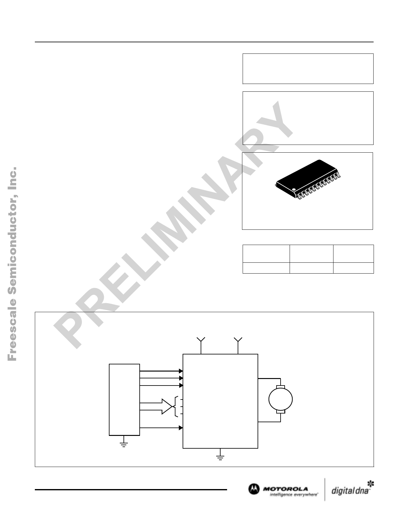
34923 Simplified Application Diagram
5.0 V
≤ 5.0 V
34923
MCU
Serial
Port
PWMMODE
DIR DCMA
PWM/ENABLE
CLOCK
DATA
STROBE
OSC
DCMB
GND
DC
Motor
This document contains information on a product under development.
Motorola reserves the right to change or discontinue this product without notice.
© Motorola, Inc. 2003
For More Information On This Product,
Go to: www.freescale.com
1 page 
Freescale Semiconductor, Inc.
STATIC ELECTRICAL CHARACTERISTICS
Characteristics noted under conditions TA = 25°C, VBB = 45 V, VDD = 5.0 V, VSENSE = 0.5 V, and fPWM < 50 kHz unless otherwise
noted.
Characteristic
Symbol Min Typ Max Unit
OUTPUT DRIVERS
Load Supply Voltage Range
Operating
During Sleep Mode
VBB V
20 – 45
0 – 45
Output Leakage Current
VOUT = VBB
VOUT = 0 V
IDSS
µA
–
<1.0
20
–
<-1.0
-20
Output On Resistance
Source Driver, IOUT = -2.0 A @ 25°C
Source Driver, IOUT = -2.0 A @ 150°C
Sink Driver, IOUT = 2.0 A @ 25°C
Sink Driver, IOUT = 2.0 A @ 150°C
RDS (ON)
–
–
–
–
mΩ
300 450
– 700
300 450
– 700
Body Diode Forward Voltage
Source Diode, IF = -2.0 A
Sink Diode, IF = 2.0 A
VF V
– 1.2 1.6
– 1.2 1.6
Load Supply Current
fPWM < 50 kHz
Charge Pump On, Outputs Disabled
Sleep Mode
IBB
– 4.0 7.0 mA
– 2.0 5.0 mA
– – 20 µA
CONTROL LOGIC
Logic Supply Voltage Range (Operating)
VDD
4.5 5.0 5.5 V
Logic Input Voltage
V
VIN(1)
2.0
–
–
VIN(0)
–
– 0.8
Input Current
All Logic Inputs Except PWM/ENABLE
VIN = 2.0 V
VIN = 0.8 V
PWM/ENABLE Only
VIN = 2.0 V
VIN = 0.8 V
IIN(1)
IIN(0)
IIN(1)
IIN(0)
µA
–
<1.0
20
–
<-2.0
-20
– 40 100
– 16 40
Input Hysteresis
All Digital Inputs Except OSC
OSC (Operating)
mV
∆VIN(LOGIC)
50
– 100
∆VIN(OSC)
200
–
400
Reference Input Voltage Range (Operating)
VREF 0 – 2.6 V
Reference Input Current
VREF = 2.5 V
IREF
µA
– – ±0.5
Input Offset Voltage
Comparator VREF = 0 V
Buffer
VIO mV
– 0 ±5.0
– 0 ±15
MOTOROLA ANALOG INTEGRATED CIRCUIT DEVICE DATA
For More Information On This Product,
Go to: www.freescale.com
34923
5
5 Page 
Freescale Semiconductor, Inc.
D14, Enable Logic
Bit D14, in conjunction with the PWM/ENABLE pin,
determines if the output drivers are in the chopped (OFF) or ON
state.
PWM/
ENABLE
0
1
1
0
D14
Operating
Mode
0
Chopped
1
0
ON
1
D15, Direction Logic
Bit D15, in conjunction with the DIR pin, determines if the
device is operating in the forward or reverse state.
State
DIR D15 DCMA DCMB
Reverse
0
1
0
Low High
1
Forward
1
0
0
High
Low
1
D16, Divisor SPAN Select
Bit D16, in conjunction with the SPAN pin, determines if VREF
is divided by 5 or 10.
Divisor
÷5
÷10
SPAN
1
0
0
1
D16
0
1
0
1
D17, Internal PWM Mode
Bit D17, in conjunction with the PWMMODE pin, selects
mixed or slow current decay.
PWMMODE
0
1
1
0
D17
Current
Decay Mode
0
Mixed
1
0
Slow
1
D18, Test Mode
Bit D18 low (default) operates the device in normal mode.
D18 is only used for testing purposes. The user should never
change this bit.
D19, Sleep Mode
Bit D19 selects a Sleep mode to minimize power
consumption when not in use. This disables much of the
internal circuitry, including the regulator and charge pump. On
power-up the serial port is initialized to all zeros. Bit D19 should
be programmed high for 1.0 ms before attempting to enable any
output driver.
D19 Sleep Mode
0 Sleep
1 Normal
Serial Port Write Timing Operations
Data is clocked into the shift register on the rising edge of the
CLOCK signal. Normally STROBE will be held high, only
brought low to initiate a write cycle. Refer to Figure 2, Serial Port
Write Timing, page 8, for the minimum timing requirements.
VREG
This internally generated voltage is used to operate the sink-
side outputs. The VREG pin should be decoupled with a 0.22 µF
capacitor to ground. VREG is internally monitored and, in the
case of a fault condition, the outputs of the device are disabled.
Charge Pump
The charge pump is used to generate a gate supply voltage
greater than VBB to drive the source-side gates. A 0.22 µF
ceramic capacitor should be connected between CP1 and CP2
for pumping purposes. A 0.22 µF ceramic capacitor should be
connected between VB and VBB to act as a reservoir to operate
the high-side devices. The VB voltage is internally monitored
and, in the case of a fault condition, the source outputs of the
device are disabled.
Shutdown
In the event of a fault (excessive junction temperature or low
voltage on VB or VREG), the outputs of the device are disabled
until the fault condition is removed. At power-up, and in the
event of low VDD, the Undervoltage Lockout circuit disables the
drivers and resets the data in the serial port to all zeros.
PWM Timer Function
The PWM timer is programmable via the serial port (bits D2–
D10) to provide off-time PWM signals to the control circuitry. In
the mixed current-decay mode, the first portion of the off time
operates in fast decay, until the fast decay time count (serial bits
D7–D10) is reached, followed by slow decay for the rest of the
off-time period (bits D2–D6). If the fast decay time is set longer
than the off time, the device effectively operates in fast decay
mode. Bit D17, in conjunction with PWMMODE, selects mixed
or slow decay.
MOTOROLA ANALOG INTEGRATED CIRCUIT DEVICE DATA
For More Information On This Product,
Go to: www.freescale.com
34923
11
11 Page | ||
| Páginas | Total 16 Páginas | |
| PDF Descargar | [ Datasheet 34923.PDF ] | |
Hoja de datos destacado
| Número de pieza | Descripción | Fabricantes |
| 34920 | Quad H-Bridge Motor Driver | Freescale Semiconductor |
| 34921 | Configurable Motor Driver IC | Freescale Semiconductor |
| 34923 | Full-Bridge PWM Motor Driver | Freescale Semiconductor |
| Número de pieza | Descripción | Fabricantes |
| SLA6805M | High Voltage 3 phase Motor Driver IC. |
Sanken |
| SDC1742 | 12- and 14-Bit Hybrid Synchro / Resolver-to-Digital Converters. |
Analog Devices |
|
DataSheet.es es una pagina web que funciona como un repositorio de manuales o hoja de datos de muchos de los productos más populares, |
| DataSheet.es | 2020 | Privacy Policy | Contacto | Buscar |