|
|
|
PDF AR6001X Data sheet ( Hoja de datos )
| Número de pieza | AR6001X | |
| Descripción | ROCm Single-Chip MAC/BB/Radio | |
| Fabricantes | Atheros | |
| Logotipo | ||
Hay una vista previa y un enlace de descarga de AR6001X (archivo pdf) en la parte inferior de esta página. Total 30 Páginas | ||
|
No Preview Available !
Data Sheet
PRELIMINARY
Revision December 2005
AR6001X ROCmTM Single-Chip MAC/BB/Radio for 2.4/5 GHz
Embedded WLAN Applications
General Description
The Atheros AR6001X is part of the AR6001
ROCm chipset family. It is a highly integrated,
all-CMOS, single chip solution for combined
cellular/handset applications and includes a 2.4/
5 GHz radio, analog-to-digital and digital-to-
analog converters, a baseband processor, multi-
protocol media access control (MAC), and a
MIPS CPU. It enables a high performance, cost
effective, low power, compact solution in a dual-
mode cellular/WLAN handset, PDA, VoIP
handset, or MP3/4 player.
The AR6001X’s transmitter combines baseband
in-phase (I) and quadrature (Q) signals, converts
them to the desired frequency, and drives the RF
signal off-chip. The receiver uses an integrated
dual-conversion architecture and requires no
off-chip intermediate frequency (IF) filters. The
frequency synthesizer supports one-MHz steps
to match the frequencies defined by IEEE 802.11
specifications. All internal clocks are generated
from a single external crystal.
The AR6001X implements half-duplex OFDM,
CCK, and DSSS baseband processing supporting
all IEEE 802.11a/g data rates. The MAC supports
the IEEE 802.11 wireless MAC protocol as well as
802.11i security, receive and transmit filtering,
error recovery, and quality of service (QoS).
The AR6001X provides multiple user interfaces
including UART, SDIO or SPI, and I2C. Other
external interfaces include serial EEPROM,
GPIOs, and LEDs.
AR6001X Features
■ All-CMOS single chip for IEEE 802.11a/g
compatible WLANs
■ Operates in 2.4 and 5 GHz frequency bands.
Freq
2.4 GHz
5 GHz
Bands
U-NII
ISM
DSRC
Europe
Japan
Frequency
2.312–2.472 GHz, 2.484 GHz
5.15–5.35 GHz, 5.725–5.825 GHz
5.725–5.850 GHz
5.850–5.925 GHz
5.15–5.35 GHz, 5.47–5.725 GHz
4.90–5.00 GHz, 5.03–5.091 GHz,
5.15–5.25, 5.25–5.35 GHz
■ Data rates of 6–54 Mbps for 802.11a and
1–54 Mbps for 802.11g
■ Integrated MIPS R4KEm CPU, clocked at up
to 141 MHz
■ 4 KB D-cache and 8 KB I-cache
■ 80 KB on-chip SRAM, 256 KB on-chip ROM
■ Stack-mounted 512 KB Flash
■ UART and serial EEPROM
■ Host interface support for SDIO/SPI, Local
Bus, or 16-bit PC Card interface
■ RTC support
■ Sleep clock using 32 KHz clock
■ Leading edge APSD support for energy
efficient operation
■ Bluetooth coexistence handshaking
■ IEEE 1149.1 standard test access port and
boundary scan architecture supported
■ Advanced power management to minimize
standby and active power
■ Standard 0.18 μm CMOS technology
■ 216-ball, 10 mm x 10 mm BGA package
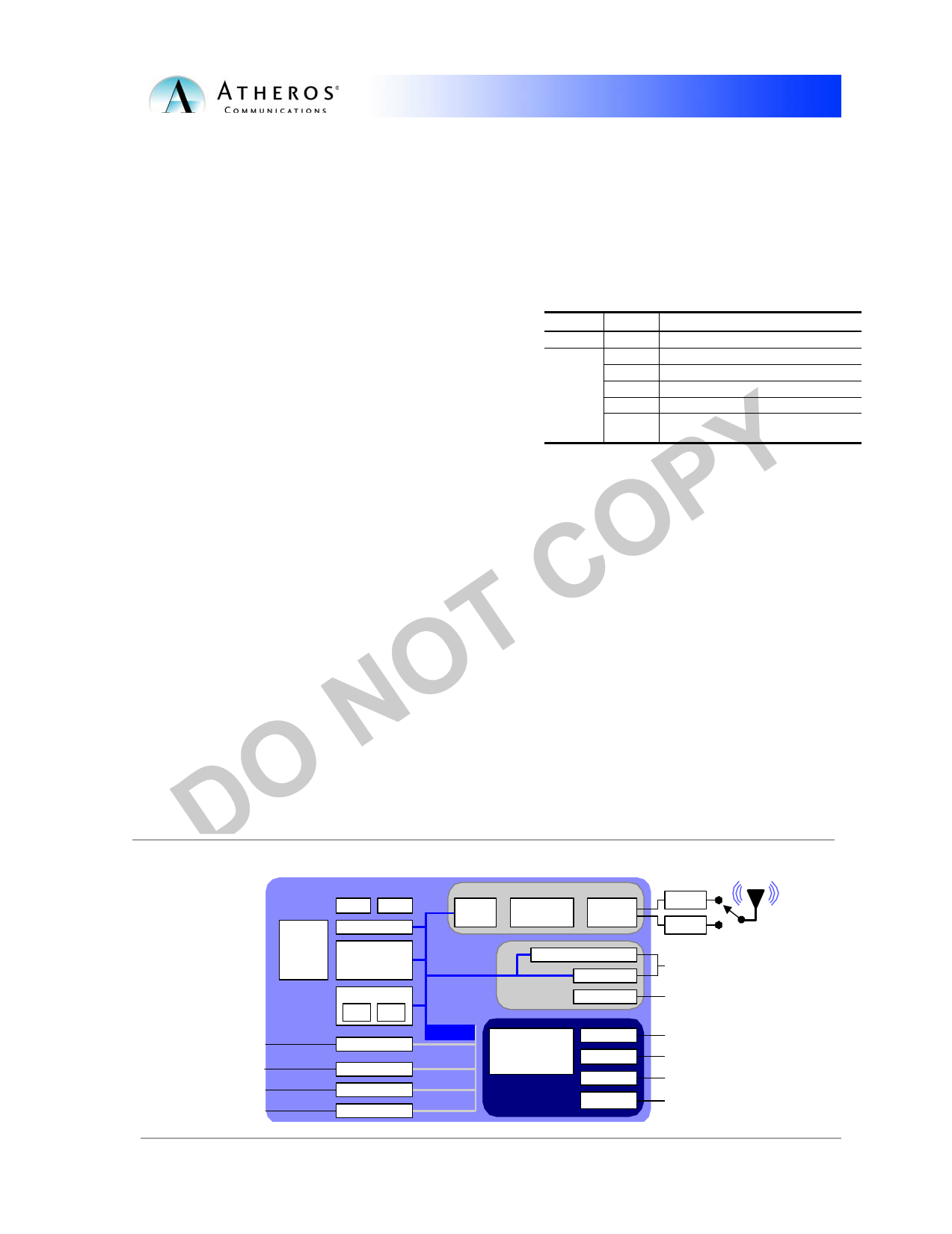
AR6001X ROCm Block Diagram
Aynchronous
Serial Interface
EEPROM/I2 S
LEDs/GPIO
I2C
AR6001
I$ D$
CPU
FLASH
DMA,
Timers,
Interrupts
Memory Control
RAM ROM
UART
SPI/Audio
GPIO
I2 C
MAC_CLK
MAC Baseband Radio
CORE_CLK
AHB
SDIO Interface
SDIO_CLK
SPI
Mem
Bridge
APB
Power, Clock
Management
LF_CLK
LDO
JTAG
REF_CLK
PA
LNA
SDIO or SPI Slave
16-bit Bus
32 KHz OSC or XTAL
1.1 – 1.8 V
Test, ICE
19.2/26/40/52 MHz
OSC or 40 MHz XTAL
© 2000-2005 by Atheros Communications, Inc. All rights reserved. Atheros™, 5-UP™, Driving the Wireless Future™, Atheros Driven™, Atheros Turbo
Mode™, and the Air is Cleaner at 5-GHz™ are trademarks of Atheros Communications, Inc. The Atheros logo is a registered trademark of
Atheros Communications, Inc. All other trademarks are the property of their respective holders.
Subject to change without notice.
COMPANY CONFIDENTIAL
•1
1 page 
PRELIMINARY
(ACG_DISABLE) 76
7.2 Memory Block Registers 77
7.2.1 Bank 0 Address
(BANK0_ADDR) 77
7.2.2 Bank 0 Configuration
(BANK0_CONFIG) 78
7.2.3 Bank 0 Read Sequence
(BANK0_READ) 79
7.2.4 Bank 0 Write Sequence
(BANK0_WRITE) 80
7.2.5 Bank 1 Address
(BANK1_ADDR) 81
7.2.6 Bank 1 Configuration
(BANK1_CONFIG) 81
7.2.7 Bank 1 Read Sequence
(BANK1_READ) 82
7.2.8 Bank 1 Write Sequence
(BANK1_WRITE) 83
7.2.9 Bank 2 Address
(BANK2_ADDR) 84
7.2.10 Bank 2 Configuration
(BANK2_CONFIG) 84
7.2.11 Bank 2 Read Sequence
(BANK2_READ) 85
7.2.12 Bank 2 Write Sequence
(BANK2_WRITE) 86
7.2.13 Interrupt When Timing Margin
Small
(TIMING_INT_ENABLE) 87
7.2.14 MC Interrupt Bits Status
(MC_ERROR_STATUS) 87
7.3 UART Registers 87
7.3.1 Receive Buffer (RBR) 88
7.3.2 Transmit Holding (THR) 88
7.3.3 Divisor Latch Low (DLL) 88
7.3.4 Divisor Latch High (DLH) 88
7.3.5 Interrupt Enable (IER) 89
7.3.6 Interrupt Identity (IIR) 89
7.3.7 FIFO Control (FCR) 89
7.3.8 Line Control (LCR) 90
7.3.9 Modem Control (MCR) 90
7.3.10 Line Status (LSR) 91
7.3.11 Modem Status (MSR) 92
7.4 Serial Interface Registers 92
7.4.1 SI Configuration
(SI_CONFIG) 93
7.4.2 SI Control/Status (SI_CS) 94
7.4.3 First Four Bytes of Tx Data
(SI_TXDATA0) 94
7.4.4 Second Four Bytes of Tx Data
(SI_TXDATA1) 95
7.4.5 First Four Bytes of Rx Data
(SI_RXDATA0) 95
7.4.6 Second Four Bytes of Rx Data
(SI_RXDATA1) 95
7.5 GPIO Registers 96
7.5.1 Drive Data Out on GPIO Pins
(GPIO_OUT) 96
7.5.2 Write 1 to Set GPIO_OUT Alias
(GPIO_OUT_W1TS) 98
7.5.3 Write 1 to Clear GPIO_OUT
Alias (GPIO_OUT_W1TC) 98
7.5.4 Enable Output Drivers for GPIO
Pins (GPIO_ENABLE) 98
7.5.5 Write 1 to Set GPIO_ENABLE
Alias
(GPIO_ENABLE_W1TS) 98
7.5.6 Write 1 to Clear GPIO_ENABLE
Alias
(GPIO_ENABLE_W1TC) 99
7.5.7 Sample Data on GPIO Pins
(GPIO_IN) 99
7.5.8 GPIO Pins Interrupt Status
(GPIO_STATUS) 99
7.5.9 Write 1 to Set GPIO_STATUS
Alias
(GPIO_STATUS_W1TS) 99
7.5.10 Write 1 to Clear GPIO_STATUS
Alias
(GPIO_STATUS_W1TC) 100
7.5.11 GPIO 0 Configuration
(GPIO_PIN0) 100
7.5.12 GPIO 1 Configuration
(GPIO_PIN1) 101
7.5.13 GPIO 2 Configuration
(GPIO_PIN2) 102
7.5.14 GPIO 3 Configuration
(GPIO_PIN3) 103
7.5.15 GPIO 4 Configuration
(GPIO_PIN4) 104
7.5.16 GPIO 5 Configuration
(GPIO_PIN5) 105
7.5.17 GPIO 6 Configuration
(GPIO_PIN6) 106
7.5.18 GPIO 7 Configuration
Atheros Communications, Inc.
COMPANY CONFIDENTIAL
AR6001X MAC/BB/Radio for Embedded WLAN Applications • 5
December 2005 • 5
5 Page 
PRELIMINARY
The AR6001’s interface bus can be configured
to be in SPI, SDIO, or Local Bus mode. Table 1-2
shows pin settings for mode configuration
using the GPIO9 and TDO pins sampled
during reset.
After reset, the particular mode set by these
pins is not changeable by software.
When the AR6001 is configured to SDIO or SPI
mode, the interface pins assume functionality
as listed under the Default column of Table 1-3.
Refer to “GPIO Registers” on page 96 for
configuration details of the GPIO pins.
Table 1-2. Pin Settings for Mode
Configuration
GPIO9
0
0
TDO
0
1
10
11
Configuration
Generic SPI Mode
SDIO Mode (Default, GPIO9
pin has weak internal pull
down, but TDO pin must be
pulled high on the board)
Local Bus Mode
Reserved
Table 1-3 shows the BGA multiplex pins (pins
that share functions).
Table 1-3. BGA Package Multiplexed Pins
Pin Local Bus Mode
B18 LB_DATA_14
C18 LB_DATA_13
D18 uses I2C_SCL0
E18 uses I2C_SDA0
F16 uses BT_ACTIVE
F17 uses RXD0
F18 uses TXD0
G17 uses RX_CLEAR
G18 uses BT_PRIORITY
H17 LB_DATA_15
H18 uses BT_FREQ
N16 LB_DATA_7
N17 LB_DATA_6
N18 LB_DATA_8
R1 LB_ADDR_5
R2 LB_ADDR_7
R18 LB_DATA_5
T1 LB_ADDR_6
T2 LB_ADDR_8
U1 LB_ADDR_9
U4 uses I2S_CK
U11 LB_INT_L
V2 LB_ADDR_10
V11 LB_WAIT_L
Default
I2S_WS
I2S_SD
I2C_SCL0
I2C_SDA0
BT_ACTIVE
RXD0
TXD0
RX_CLEAR
BT_PRIORITY
I2S_MCK
BT_FREQ
LB_DATA_7
LB_DATA_6
LB_DATA_8
SDIO_CMD
SDIO_DATA_2
LB_DATA_5
SDIO_DATA_3
SDIO_DATA_1
SDIO_DATA_0
I2S_CK
LB_INT_L
SDIO_CLK
LB_WAIT_L
SDIO/SPI Mode
GPIO
GPIO10
GPIO11
GPIO0
GPIO1
GPIO4
GPIO3
GPIO2
GPIO6
GPIO5
GPIO8
GPIO7
GPIO17
GPIO16
GPIO12/UART_CTS_L[1]
GPIO15
GPIO9
GPIO14/UART_CLK[3]
GPIO13/UART_RTS_L[4]
[1]See the register “GPIO 12 Configuration (GPIO_PIN12)” on page 112 for more information.
[2]Duplicate for flexibility.
[3]See the register “GPIO 14 Configuration (GPIO_PIN14)” on page 114 for more information.
[4]See the register “GPIO 13 Configuration (GPIO_PIN13)” on page 113 for more information.
SPI Master
SPI_CK
SPI_MISO
SPI_MOSI
SPI_CS0_L
Reserved
Reserved
SPI_CS0_L[2]
G_SPI_MOSI
Reserved
G_SPI_CS
G_SPI_INT
G_SPI_MISO
G_SPI_CLK
SPI_MOSI[2]
Atheros Communications, Inc.
COMPANY CONFIDENTIAL
AR6001X MAC/BB/Radio for Embedded WLAN Applications • 11
December 2005 • 11
11 Page | ||
| Páginas | Total 30 Páginas | |
| PDF Descargar | [ Datasheet AR6001X.PDF ] | |
Hoja de datos destacado
| Número de pieza | Descripción | Fabricantes |
| AR6001X | ROCm Single-Chip MAC/BB/Radio | Atheros |
| Número de pieza | Descripción | Fabricantes |
| SLA6805M | High Voltage 3 phase Motor Driver IC. |
Sanken |
| SDC1742 | 12- and 14-Bit Hybrid Synchro / Resolver-to-Digital Converters. |
Analog Devices |
|
DataSheet.es es una pagina web que funciona como un repositorio de manuales o hoja de datos de muchos de los productos más populares, |
| DataSheet.es | 2020 | Privacy Policy | Contacto | Buscar |