|
|
PDF 32LD330H Data sheet ( Hoja de datos )
| Número de pieza | 32LD330H | |
| Descripción | LCD TV SERVICE MANUAL | |
| Fabricantes | LG | |
| Logotipo |  |
|
Hay una vista previa y un enlace de descarga de 32LD330H (archivo pdf) en la parte inferior de esta página. Total 30 Páginas | ||
|
No Preview Available !
North/Latin America
Europe/Africa
Asia/Oceania
Internal Use Only
http://aic.lgservice.com
http://eic.lgservice.com
http://biz.lgservice.com
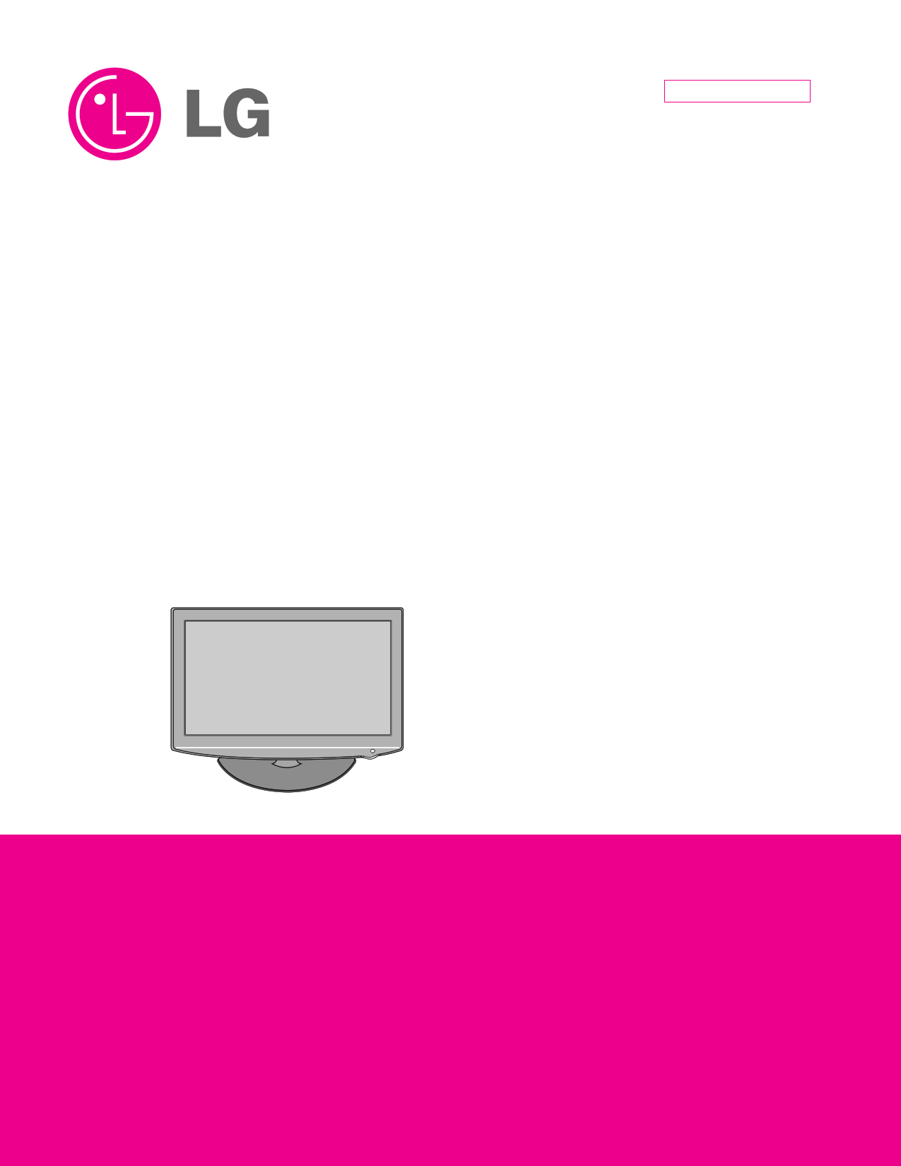
LCD TV
SERVICE MANUAL
CHASSIS : LA06H
MODEL : 32LD340H 32LD340H-UA
MODEL : 32LD330H 32LD330H-UA
CAUTION
BEFORE SERVICING THE CHASSIS,
READ THE SAFETY PRECAUTIONS IN THIS MANUAL.
P/NO : MFL67207503 (1106-REV00)
Printed in Korea
1 page 
IC Remove/Replacement
Some chassis circuit boards have slotted holes (oblong) through
which the IC leads are inserted and then bent flat against the
circuit foil. When holes are the slotted type, the following technique
should be used to remove and replace the IC. When working with
boards using the familiar round hole, use the standard technique
as outlined in paragraphs 5 and 6 above.
Removal
1. Desolder and straighten each IC lead in one operation by gently
prying up on the lead with the soldering iron tip as the solder
melts.
2. Draw away the melted solder with an anti-static suction-type
solder removal device (or with solder braid) before removing the
IC.
Replacement
1. Carefully insert the replacement IC in the circuit board.
2. Carefully bend each IC lead against the circuit foil pad and
solder it.
3. Clean the soldered areas with a small wire-bristle brush.
(It is not necessary to reapply acrylic coating to the areas).
"Small-Signal" Discrete Transistor
Removal/Replacement
1. Remove the defective transistor by clipping its leads as close as
possible to the component body.
2. Bend into a "U" shape the end of each of three leads remaining
on the circuit board.
3. Bend into a "U" shape the replacement transistor leads.
4. Connect the replacement transistor leads to the corresponding
leads extending from the circuit board and crimp the "U" with
long nose pliers to insure metal to metal contact then solder
each connection.
Power Output, Transistor Device
Removal/Replacement
1. Heat and remove all solder from around the transistor leads.
2. Remove the heat sink mounting screw (if so equipped).
3. Carefully remove the transistor from the heat sink of the circuit
board.
4. Insert new transistor in the circuit board.
5. Solder each transistor lead, and clip off excess lead.
6. Replace heat sink.
Diode Removal/Replacement
1. Remove defective diode by clipping its leads as close as
possible to diode body.
2. Bend the two remaining leads perpendicular y to the circuit
board.
3. Observing diode polarity, wrap each lead of the new diode
around the corresponding lead on the circuit board.
4. Securely crimp each connection and solder it.
5. Inspect (on the circuit board copper side) the solder joints of
the two "original" leads. If they are not shiny, reheat them and if
necessary, apply additional solder.
Fuse and Conventional Resistor
Removal/Replacement
1. Clip each fuse or resistor lead at top of the circuit board hollow
stake.
2. Securely crimp the leads of replacement component around
notch at stake top.
3. Solder the connections.
CAUTION: Maintain original spacing between the replaced
component and adjacent components and the circuit board to
prevent excessive component temperatures.
Circuit Board Foil Repair
Excessive heat applied to the copper foil of any printed circuit
board will weaken the adhesive that bonds the foil to the circuit
board causing the foil to separate from or "lift-off" the board. The
following guidelines and procedures should be followed whenever
this condition is encountered.
At IC Connections
To repair a defective copper pattern at IC connections use the
following procedure to install a jumper wire on the copper pattern
side of the circuit board. (Use this technique only on IC
connections).
1. Carefully remove the damaged copper pattern with a sharp
knife. (Remove only as much copper as absolutely necessary).
2. carefully scratch away the solder resist and acrylic coating (if
used) from the end of the remaining copper pattern.
3. Bend a small "U" in one end of a small gauge jumper wire and
carefully crimp it around the IC pin. Solder the IC connection.
4. Route the jumper wire along the path of the out-away copper
pattern and let it overlap the previously scraped end of the good
copper pattern. Solder the overlapped area and clip off any
excess jumper wire.
At Other Connections
Use the following technique to repair the defective copper pattern
at connections other than IC Pins. This technique involves the
installation of a jumper wire on the component side of the circuit
board.
1. Remove the defective copper pattern with a sharp knife.
Remove at least 1/4 inch of copper, to ensure that a hazardous
condition will not exist if the jumper wire opens.
2. Trace along the copper pattern from both sides of the pattern
break and locate the nearest component that is directly
connected to the affected copper pattern.
3. Connect insulated 20-gauge jumper wire from the lead of the
nearest component on one side of the pattern break to the lead
of the nearest component on the other side.
Carefully crimp and solder the connections.
CAUTION: Be sure the insulated jumper wire is dressed so the
it does not touch components or sharp edges.
Copyright
LG Electronics. Inc. All right reserved.
Only for training and service purposes
-5-
LGE Internal Use Only
5 Page 
ADJUSTMENT INSTRUCTION
1. Application range
This spec. sheet applies to LA06G Chassis applied LCD TV
all models manufactured in TV factory
2. Specification
2.1 Because this is not a hot chassis, it is not necessary
to use an isolation transformer. However, the use of
isolation transformer will help protect test instrument.
2.2 AdjThe adjustment must be performed in the
circumstance of 25 ±5 C of temperature and
65±10% of relative humidity if there is no specific
designation.
2.4 The input voltage of the receiver must keep
100~240V, 50/60Hz.
2.5 The receiver must be operated for about 5 minutes
prior to the adjustment when module is in the
circumstance of over 15
In case of keeping module is in the circumstance of
0°C, it should be placed in the circumstance of above
15°C for 2 hours
In case of keeping module is in the circumstance of
below -20°C, it should be placed in the circumstance of
above 15°C for 3 hours,.
Caution) When still image is displayed for a period of 20
minutes or longer (especially where W/B scale is
strong. Digital pattern 13ch and/or Cross hatch
pattern 09ch), there can some afterimage in the
black level area.
3. Adjustment items
3.1 Board Level Adjustment
• Adjust 480i Comp1 (ADC)
• EDID/DDC download
Above adjustment items can be also performed in Final
Assembly if needed. Both Board-level and Final assembly
adjustment items can be check using In-Star Menu 1.ADJUST
CHECK.
Component 1080p RGB-PC Adjust will be calculated by 480i
adjust value.
3.2 Final assembly adjustment
• White Balance adjustment
• RS-232C functionality check
• Factory Option setting per destination
• Ship-out mode setting (In-Stop)
3.3 Etc
• Ship-out mode
• Tool option menu
• USB Download(S/W Update, Option, Service only)
• ISP Download(Option)
4. Automatic Adjustment
4.1. ADC Adjustment
(1) Overview
ADC adjustment is needed to find the optimum black level
and gain in Analog-to-Digital device and to compensate
RGB deviation.
(2) Equipment & Condition
1) Jig (RS-232C protocol)
2) Inner Pattern
- Resolution : 1080P (Inner Pattern)
- Resolution : 1024*768 RGB (Inner Pattern)
- Pattern : Horizontal 100% Color Bar Pattern
- Pattern level : 0.7±0.1 Vp-p
(3) Adjustment
1) Adjustment method
- Using RS-232, adjust items listed in 3.1 in the other
shown in “4.1.3.3”
2) Adj. protocol
Ref.) ADC Adj. RS232C Protocol_Ver1.0
3) Adj. order
Protocol
Command
Set ACK
Enter adj. mode aa 00 00 a 00 OK00x
Source change xb 00 40 b 00 OK40x (Adjust 480i Comp1 )
xb 00 60 b 00 OK60x (Adjust 1080p RGB)
Begin adj.
ad 00 10
Return adj. result
OKx (Case of Success)
NGx (Case of Fail)
Read adj. data (main)
(main)
ad 00 20 000000000000000000000000007c007b006dx
(sub)
(sub)
ad 00 21 000000070000000000000000007c00830077x
Confirm adj.
ad 00 99 NG 03 00x (Fail)
NG 03 01x (Fail)
NG 03 02x (Fail)
OK 03 03x (Success)
End adj.
aa 00 90 a 00 OK90x
- aa 00 00 [Enter ADC adj. mode]
- xb 00 40 [Change input source to Component1(480i)]
- ad 00 10 [Adjust 480i Comp1]
- xb 00 60 [Change input source to RGB(1024*768)]
- ad 00 10 [Adjust 1024*768 RGB]
- ad 00 90 End adj.
Copyright
LG Electronics. Inc. All right reserved.
Only for training and service purposes
- 11 -
LGE Internal Use Only
11 Page | ||
| Páginas | Total 30 Páginas | |
| PDF Descargar | [ Datasheet 32LD330H.PDF ] | |
Hoja de datos destacado
| Número de pieza | Descripción | Fabricantes |
| 32LD330 | LCD TV SERVICE MANUAL | LG |
| 32LD330-MA | LCD TV SERVICE MANUAL | LG |
| 32LD330H | LCD TV SERVICE MANUAL | LG |
| Número de pieza | Descripción | Fabricantes |
| SLA6805M | High Voltage 3 phase Motor Driver IC. |
Sanken |
| SDC1742 | 12- and 14-Bit Hybrid Synchro / Resolver-to-Digital Converters. |
Analog Devices |
|
DataSheet.es es una pagina web que funciona como un repositorio de manuales o hoja de datos de muchos de los productos más populares, |
| DataSheet.es | 2020 | Privacy Policy | Contacto | Buscar |
